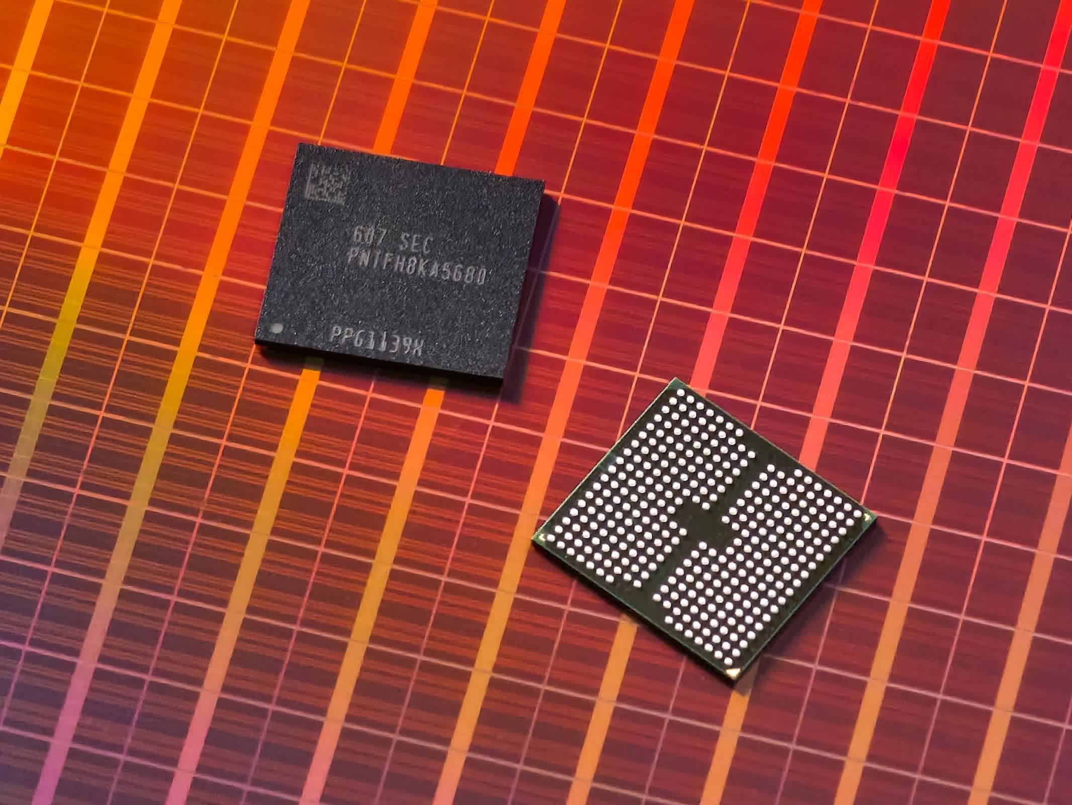
Samsung Electronics unveiled three next-generation memory technologies at the Future of Memory and Storage (FMS) 2026 conference in Santa Clara on August 5, aiming to address the growing memory bottleneck in AI data centers.
The centerpiece, zHBM, stacks high-bandwidth memory directly on top of AI accelerator chips instead of placing it beside them, a design Samsung says will deliver roughly 8x the performance and more than 10x the density of today's HBM5, alongside a 3x gain in energy efficiency and over 50% lower thermal resistance. zNAND-O, a companion NAND technology in four- and eight-layer versions, targets low-latency edge AI applications.
Samsung's V10 BV-NAND takes a different approach, using wafer-bonding technology to pack more than 400 individual flash layers into a single chip — about 58% denser than its V9 predecessor, with faster read, write, and I/O speeds. zHBM and zNAND-O remain concept models rather than shipping products, but the announcement signals where Samsung expects the memory industry to head as AI workloads demand ever more bandwidth close to the processor.