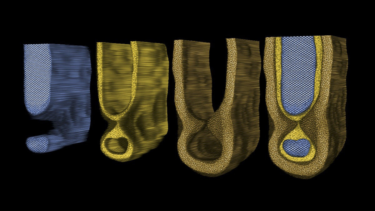
A Cornell-led research team has achieved the first atomic-scale 3D images of defects lurking inside modern computer chips. Using electron ptychography — a technique that fires electrons through transistor layers and computationally reconstructs the scattering patterns — doctoral student Shake Karapetyan and professor David Muller revealed irregular formations they dubbed "mouse bites" along the walls of transistor channels just 15 to 18 atoms wide.
The imaging method, developed in collaboration with TSMC and Advanced Semiconductor Materials (ASM), uses Cornell's electron microscope pixel array detector (EMPAD), which holds the Guinness World Record for highest-resolution images of atoms. The research, published in Nature Communications, shows that these previously invisible interface roughness defects can degrade chip performance in ways manufacturers couldn't detect until now.
The breakthrough has implications for virtually every device with a modern processor — from smartphones to AI data centers — and could prove especially valuable for debugging next-generation quantum computers, which demand extraordinary structural precision at the atomic level.